|
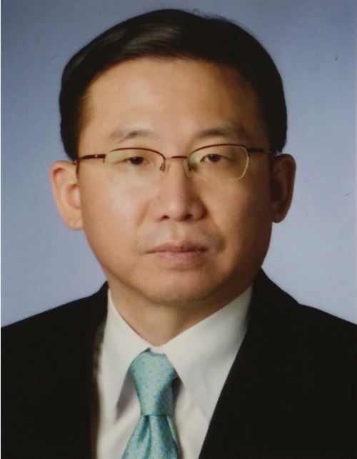
Chiwoo Kim APS Holdings, President & CTO |
|
Biography Education History: - Post Doctoral Research Fellow: Jan. University of Michigan, Ann Arbor, 1991 - M.A. and Ph.D. in Condensed Matter Physics, Univ. of Texas at Austin, 1989 - B.S. in Physics, Yonsei University, Seoul, Korea, 1984 Professional History: - President & CTO: APS Holdings, Jan. 2018 - Present . Executive Vice President: AP Systems, Feb. 2016 - Dec. 2017, - Visiting, Adjunct Professor: Seoul National University: Sep. 2015 - Aug. 2018, Electrical & Computer Engineering - Samsung Group: Aug. 1991 - Dec. 2014 . Head of A3 Flexible OLED Line Construction: Senior VP of Samsung Display, Jan. 2012 - Dec. 2014, . Head of AMOLED R&D: VP of Samsung Mobile Display, Feb. 2009 - Dec. 2012 . R&D of Backplane Technology: VP of Samsung Electronics, Aug. 1991 - Dec. 2008 - Adjunct Professor: Sungkyunkwan University, Sep. 2000 - Dec. 2014 Electrical Engineering Department Abstract Two key issues of the flexible OLED are the TFE (thin film encapsulation) process and the patterning process for UHD or higher resolution (>800ppi). First, ALD (atomic layer deposition) based TFE solution is introduced. TFE process is extremely complicated and needs so many know-hows to pass the severe reliability tests. AP Systems introduces the inorganic and organic sandwich structure process for the next generation Foldable TFE solution. Second, 800ppi high resolution FMM process is explained. APS Holdings’ solution for RGB patterning is the high accuracy fine metal mask (FMM). To implement the UHD or higher resolution displays, specially designed and fabricated FMM should be developed. The technical hurdles and the solutions of the FMM materials and patterning process are discussed. |
|
